Product Number:S460
Product Usage:JHIMS 460 solder paste inspection machine is mainly used to inspect the printing quality of solder paste on PCB to ensure that the solder paste quantity and distribution meet the requirements.
Applicable Industries:JHIMS 460 solder paste inspection machine is widely used in electronic manufacturing, communications, automotive electronics, consumer electronics, medical electronics and industrial control industries to ensure the printing quality of PCB solder paste.

National Advisory Hotline:
+86 18975335491
In SMT assembly, precise solder paste deposition prevents up to 70% of defects. The JHIMS S460 uses innovative PSLM PMP technology for shadow-free 3D measurements, boosting first-pass yields by 20% in high-volume PCB production. As a leader in SMT inspection since 2005, Shenzhen Jinghe Technology delivers reliable solutions for global electronics manufacturing.
Traditional 2D SPI misses volume inaccuracies, leading to reflow failures. Our 3D SPI machine captures true height profiles with <1μm repeatability, integrating PSLM technology for zero mechanical wear. In 2025's miniaturized era, AI warp prediction analyzes PCB trends proactively, cutting inspection time by 15% over competitors like Viscom or Yamaha.
LSI Optimization Tip: Focus on "SMT defect reduction" to align with rising queries for yield improvement in volatile markets.
Engineered for 24/7 operation, the S460 combines patented D-Lighting for full-spectrum detection with Stop & Catch multi-imaging, ensuring <1% measurement variance even on warped boards.
| Parameter | Description | Value |
|---|---|---|
| Series | Model Type | S460 Cost-Effective |
| Measurement Principle | Core Tech | 3D White Light PSLM PMP (Moiré Fringe) |
| Key Measurements | Metrics | Volume, Area, Height, XY Offset, Shape |
| Detection Types | Defects | Missing Print, Insufficient/Excessive Tin, Bridging, Offset, Contamination |
| Camera | Pixel/Optics | 5M; Telecentric + Coaxial Light |
| Resolution | Lens Detail | 16μm/13μm |
| Min Element | Support | British 0201 |
| Accuracy | XY/Height | 1μm / 0.37μm |
| Repeatability (3σ) | Precision | Height: <1μm; Volume/Area: <1% |
| Gage R&R | Variability | <10% |
| FOV Speed | Efficiency | 0.45s per Field |
| Heads | Config | Single |
| RGB Lighting | Standard | Included |
| Mark Detection | Time | 0.5s/piece |
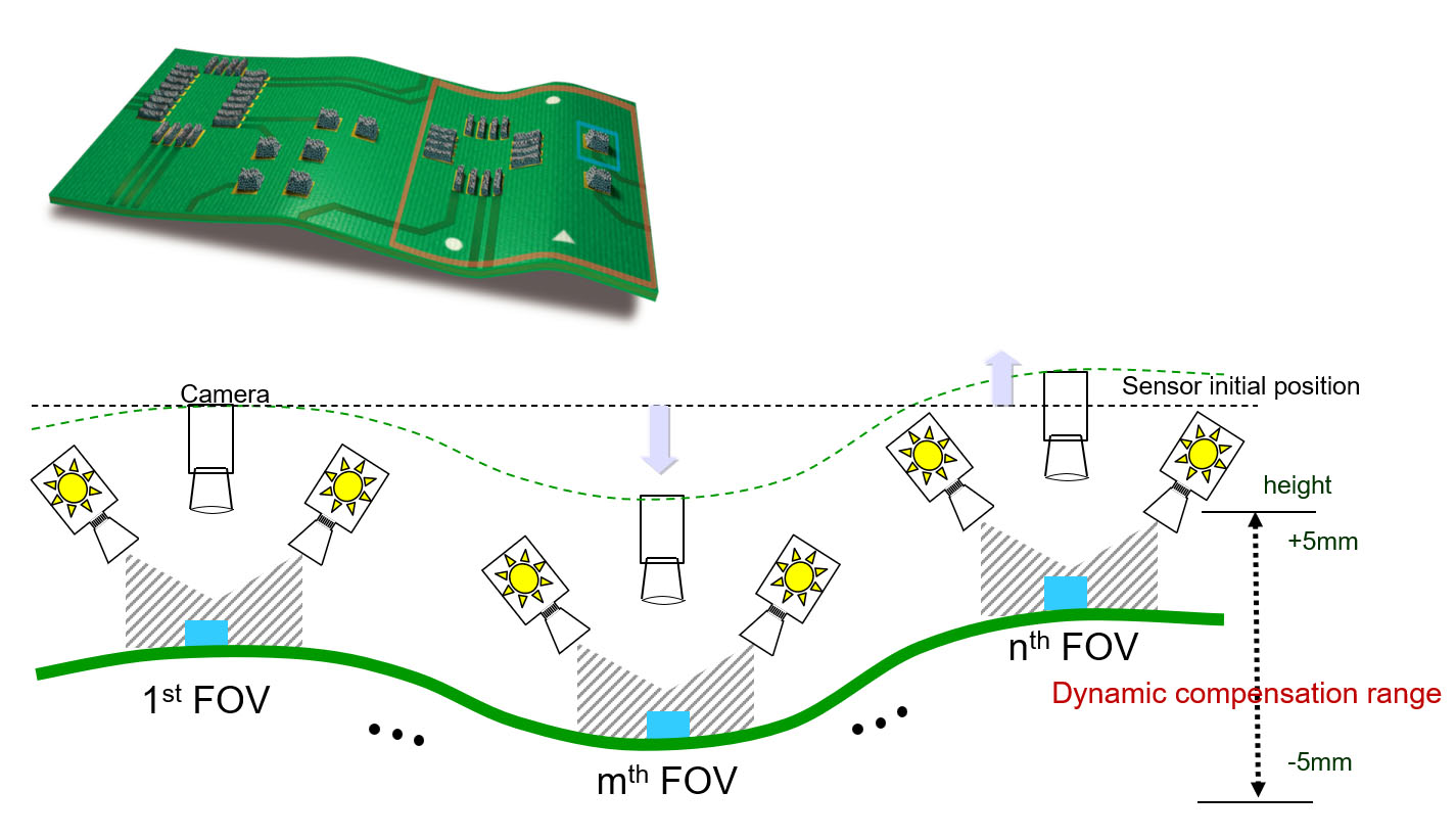
| Warp Compensation | Z-Axis | Standard (±5mm) |
| Max Height | Range | ±550μm (±1200μm Option) |
| Min Pad | Spacing | 150μm |
| Max PCB | Size/Thickness | 460x460mm / 0.4-7mm |
| Part Heights | Limits | Up: 30mm; Down: 40mm |
| Edge Distance | Board | 3mm (Clip Option) |
| Orbit | Setup | Front (Back Option) |
| Transfer Dir. | Flexible | L-R or R-L; Manual/Auto Adjust |
| SPC Tools | Analytics | Histogram, Xbar-R/S, CP/CPK, Reports |
| Data Input | Gerber/CAD | 274x/D; Teach Mode; X/Y Import |
| CPU/RAM/GPU | IPC | i7 / 24G (32G Opt) / 2G (4G Opt) |
| Storage/OS | Config | 1TB SSD / Windows 10 Pro 64-bit |
| Dimensions/Weight | Footprint | 1000x1150x1525mm / 965kg |
| Power/Air | Req. | 220V 10A / 4-6 Bar |
| Usage | Start/Normal | 2.5kW / 2kW |
| Floor Load | Min. | 600kg/m² |
| Options | Add-Ons | Barcode, Offline Prog., UPS, Ultrasonic |
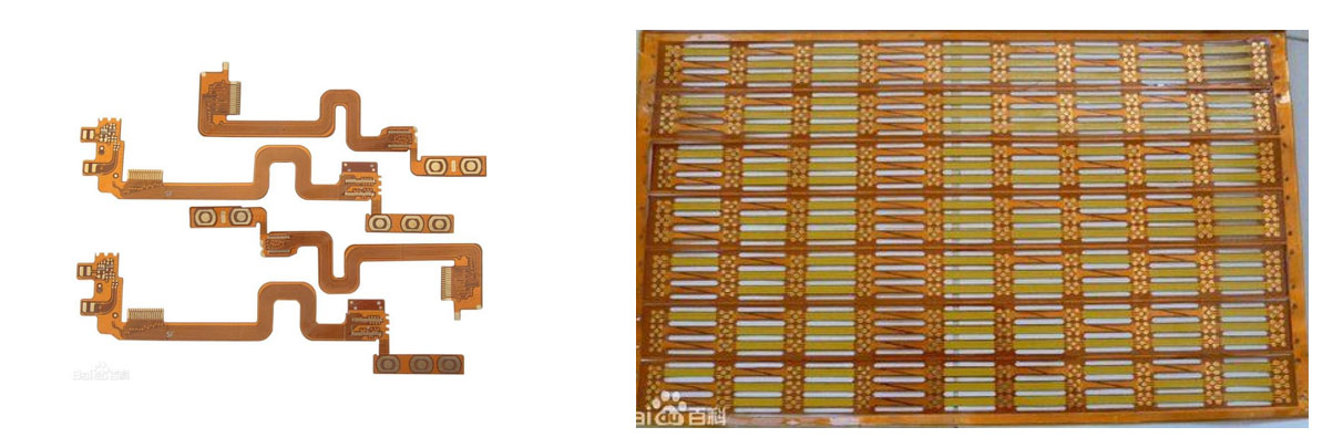
Warpage impacts 30% of SMT runs; S460's AI-driven Z-axis profiles per-FOV, compensating ±5mm dynamically—essential for FPCs in wearables. Unlike static systems, our PSLM tech predicts distortions via ML algorithms, reducing false positives by 25%.

From flexible substrates to rigid boards, achieve sub-micron accuracy. Deep Dive: Warp Challenges in SMT.

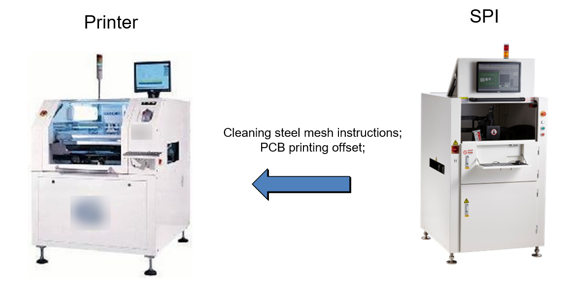
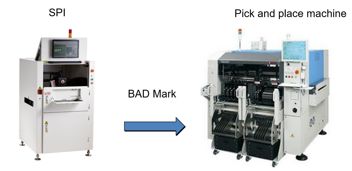
Boost efficiency: S460 shares badmark data with placers, skipping defects to save 30% mounting time. Printer feedback auto-cleans stencils post-missing prints—proven with GKG/Desen models.

Barcode-enabled for multi-run traceability. Full M2M Solutions Guide.

Deploy S460 in automotive (EV battery PCBs), medical (implant sensors), and consumer 5G modules for high-reliability needs. It excels in jet-printing vs. screen, handling 50% faster inspections per TRI benchmarks.
Case Study: A 2025 Shenzhen firm integrated S460 into their SMT line, yielding 25% defect drop and 6-month ROI via 15% throughput gain—CPK from 1.2 to 1.8.
"Transformed our yields—essential for scaling production." — Lead Engineer, TechCorp (150+ installs).
Interactive ROI Tool: Estimate savings based on your volume. Calculate Now.
LSI Expansion: Integrate with AOI for end-to-end "SMT defect reduction," aligning with Industry 4.0 trends like predictive maintenance.
© 2025 Shenzhen Jinghe Technology Co., Ltd.(JHIMS)| Sitemap
