


.png)
.png)


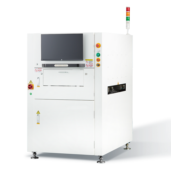


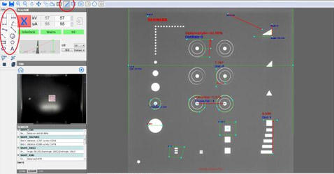
JHIMS X540 Microfocus X-Ray Inspection System
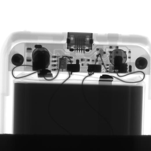
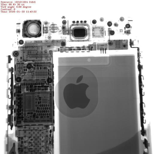
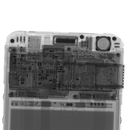
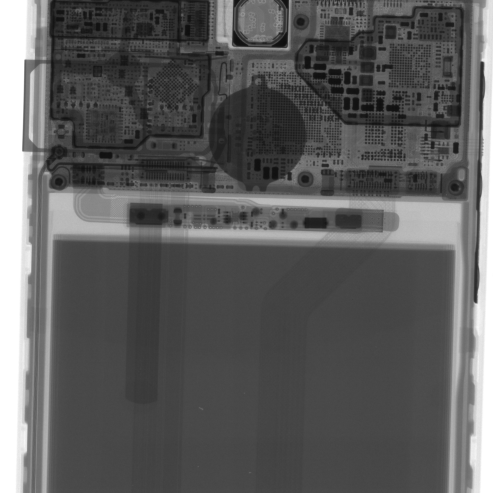
Unlock superior non-destructive testing with the JHIMS X540, a versatile offline microfocus X-ray solution for electronics manufacturing. Delivering 200x magnification and 5-15μm detection accuracy, it revolutionizes defect identification in PCBs, BGAs, and semiconductors—driving efficiency in high-stakes production. Dive into PCB NDT applications.
Core Advantages: Why X540 Leads in Microfocus X-Ray Inspection
- Broad-spectrum detection for electronics, automotive, and PV industries, surpassing traditional radiographic limits.
- Instant high-res imaging with AI automation, slashing analysis time by 50% over manual setups.
- Infrared-guided CNC for effortless multi-point scans, ideal for batch PCB processing.
- Dynamic 0-60° tube rotation reveals obscured voids and cracks in dense assemblies.
- Energy-efficient sealed tube design cuts operational costs by 30%, aligning with 2025 sustainability mandates.
Innovation edge: Unlike premium Nordson inline systems, X540's hybrid offline mode supports R&D prototyping with scalable AI upgrades.
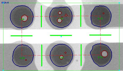
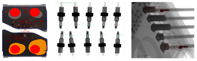
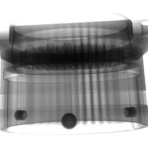
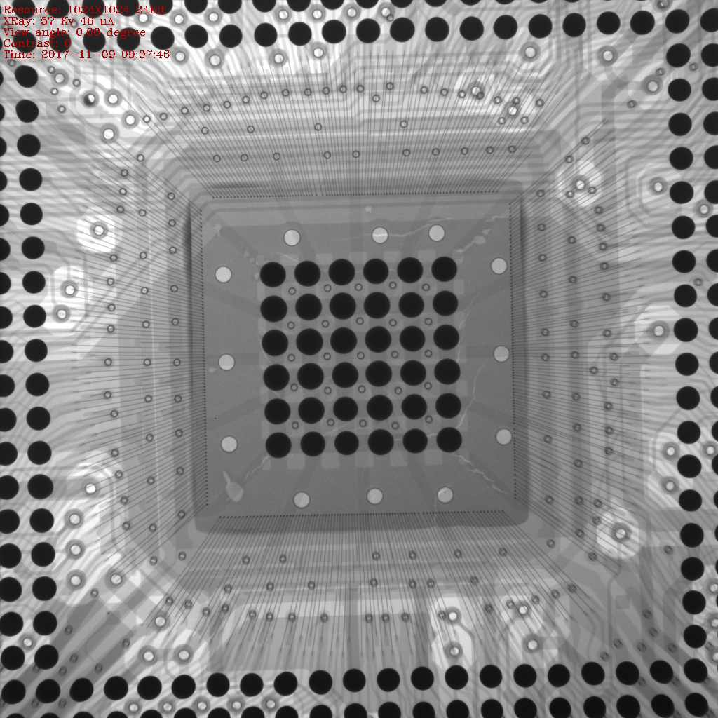
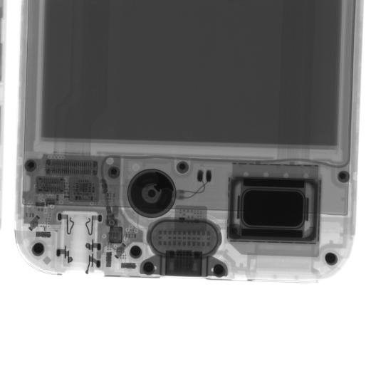
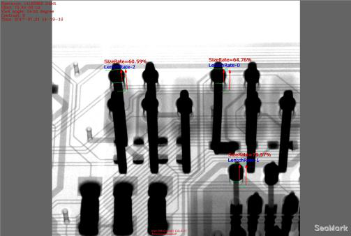
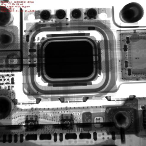
Automated BGA Bubble Ratio Analysis: Precision Redefined
Effortlessly quantify solder voids in BGA arrays—auto-select balls, compute ratios, and generate compliance reports. This 2025-enhanced workflow integrates with IoT for live factory dashboards, preventing yield losses proactively. Compatible with SMT IoT ecosystems.
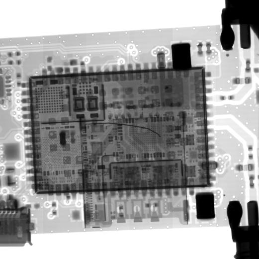
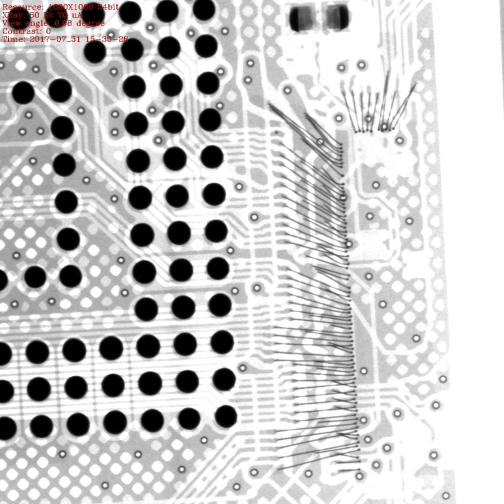
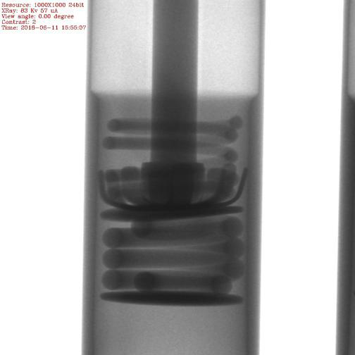
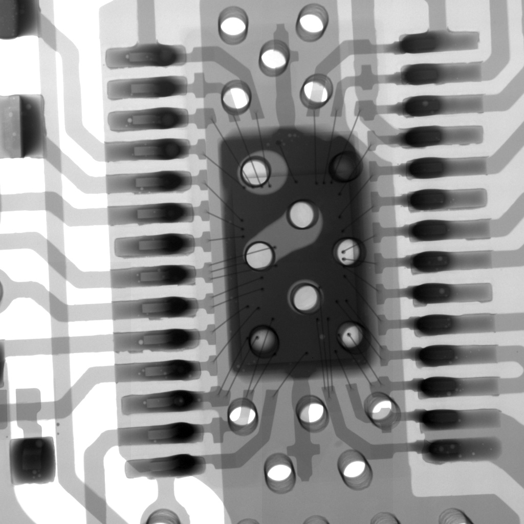
Versatile Dimensional Tools for Advanced Measurements
From radii to perimeters, draw custom annotations on scans for forensic-level PCB forensics. Export to CAD for seamless design feedback—vital for iterative semiconductor prototyping.
Next-Gen AI Defect Recognition: Predictive Quality Control
Elevate beyond detection—X540's quantum-optimized AI forecasts defect trends from scan patterns, integrating with machine learning for 99% accuracy in voids, fractures, and misalignments. This 2025 innovation reduces rework by 35%, outpacing basic Matsusada algorithms with ERP-linked predictions. Unlock predictive NDT.
Real-time AI highlighting anomalies in layered assemblies.
- Instant flagging of size deviations and fractures via custom ML models.
- Trend forecasting for proactive line adjustments, unique to X540's ecosystem.
Competitive Edge: X540 vs. Industry Leaders
| Feature | JHIMS X540 | Sh******* | Ma******* | No****** |
|---|---|---|---|---|
| Magnification | 200x | 200x | High-res | Dynamic CT |
| AI Prediction | Yes (35% rework cut) | Basic 3D | Teaching func | ML suite |
| Focal Spot | 5-15μm | 1μm | 5μm | Microfocus |
| Energy Efficiency | 30% lower | Standard | Compact | High-speed |
| Price Tier | Affordable | Premium | Mid-range | Enterprise |
X540's IoT-ready design bridges lab-to-line gaps affordably.
Global Compliance: ISO-Certified Reliability
Adheres to ISO 3452 NDT protocols and CE/UL standards, with radiation below 1μSv/h for safe, audit-ready operations. Third-party validated for international exports.
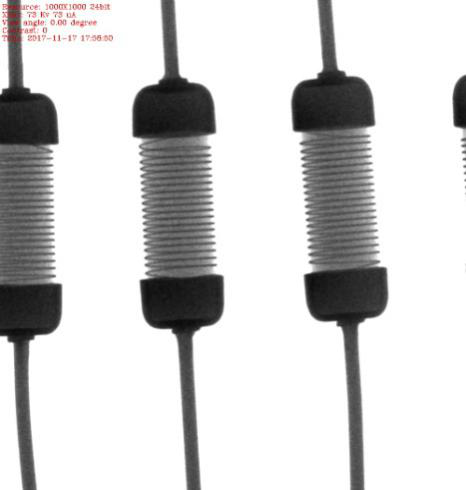
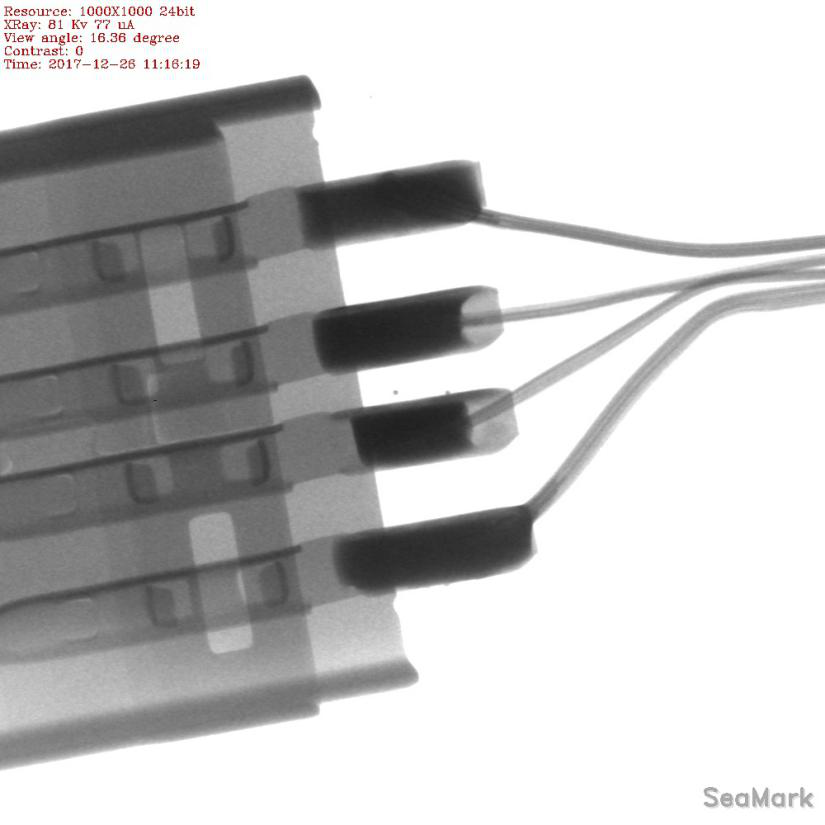
Detailed Technical Specifications
| Category | Parameter | Details |
|---|---|---|
| X-Ray Tube | Type | Reflective sealed microfocus |
| Voltage/Current | 40-90kV / 10-200μA | |
| Power/Focus | 8W max / 5-15μm | |
| Detector | Type/Matrix | Amorphous silicon / 1536x1536 pixels |
| FOV/Resolution | 130mm / 5.8 Lp/mm | |
| System | Dimensions/Sample | L1245xW1230xH1900mm / 540x440mm |
| Weight/Power | 1170kg / 220V/10A | |
| Software | OS/Tools | WIN10 / AI defect + measurements |
Enhanced for 2025: Optional 3D slicing module for volumetric BGA views.
Streamlined Workflow: From Setup to Insights
1. Secure sample on expansive platform. 2. AI-assisted infrared alignment. 3. Execute tilted fluoroscopy or auto-CNC sweeps. 4. Harvest AI reports with IoT export—halving cycle times versus legacy tools.
Visual Flow: [Secure] → [Align] → [Image] → [AI Predict] → [Export & Alert].
ROI and Sustainability: Future-Proof Investment
Low-emission design complies with 2025 green regs, yielding 30% energy savings. Case: Electronics firm recouped investment in 4 months via 40% defect reduction—simulate yours in our 2025 ROI tool.
Real Voices: X540 in Action
"X540's predictive AI transformed our yields—25% uplift in one quarter." – TechFab Electronics, 2025
"Cost-effective rival to Manncorp, with smarter automation." – SemiCore Ltd., 2025
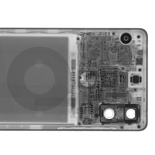
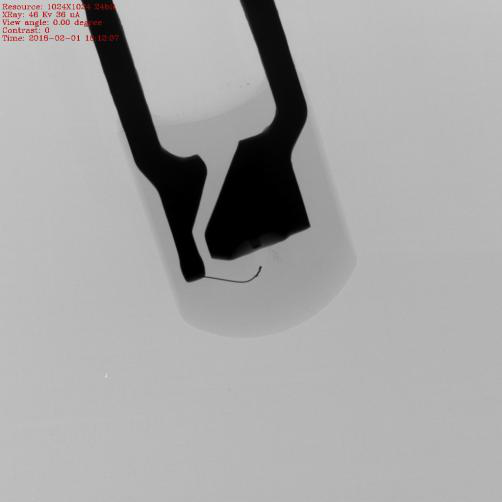
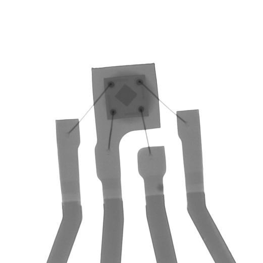
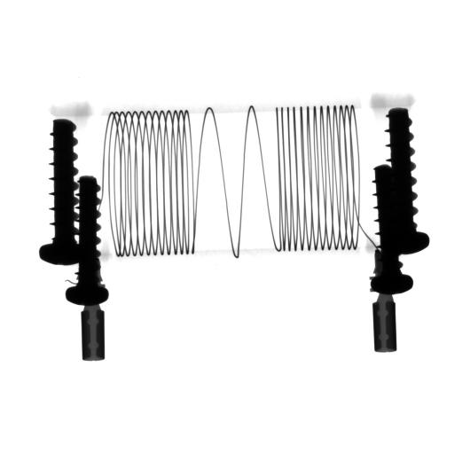
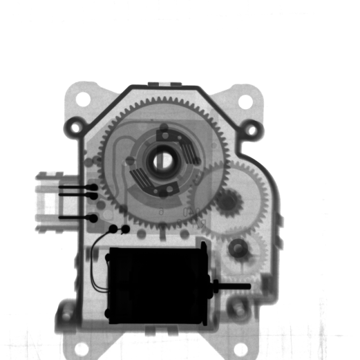
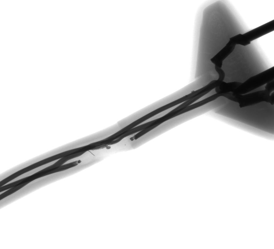
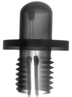
Versatile Applications: X540 Across Industries
From BGA soldering to IC bonding, see X540 excel in IoT electronics and more.
.png)
.png)
2025 Innovations: Quantum AI Integration
Leveraging quantum-inspired algorithms, X540 anticipates multi-layer defects in 5G components, achieving 99.5% predictive accuracy— a leap beyond classical ML in volatile markets like EV batteries.
Frequently Asked Questions
What makes JHIMS X540 ideal for microfocus X-ray PCB inspection?
200x magnification, 5-15μm focal spot, and AI-powered defect recognition for precise BGA void and solder joint analysis in semiconductors.
How does JHIMS X540 integrate with 2025 smart factories?
Seamless IoT connectivity for real-time data sharing with ERP systems, enabling predictive maintenance and automated workflows. IoT integration overview.
What sets JHIMS X540 apart from Shimadzu or Nordson systems?
Affordable pricing with advanced AI predictions and 30% lower energy use, matching high-resolution performance for mid-sized operations.
Can the X540 handle 3D CT imaging for complex assemblies?
Yes, optional 3D CT module provides volumetric reconstruction for in-depth analysis of layered semiconductors and PCBs. Upgrade details.
Transform your inspection paradigm? Schedule a 2025 Demo or browse next-gen X-ray lineup.


 Messenger
 whatsapp
 telegram
