

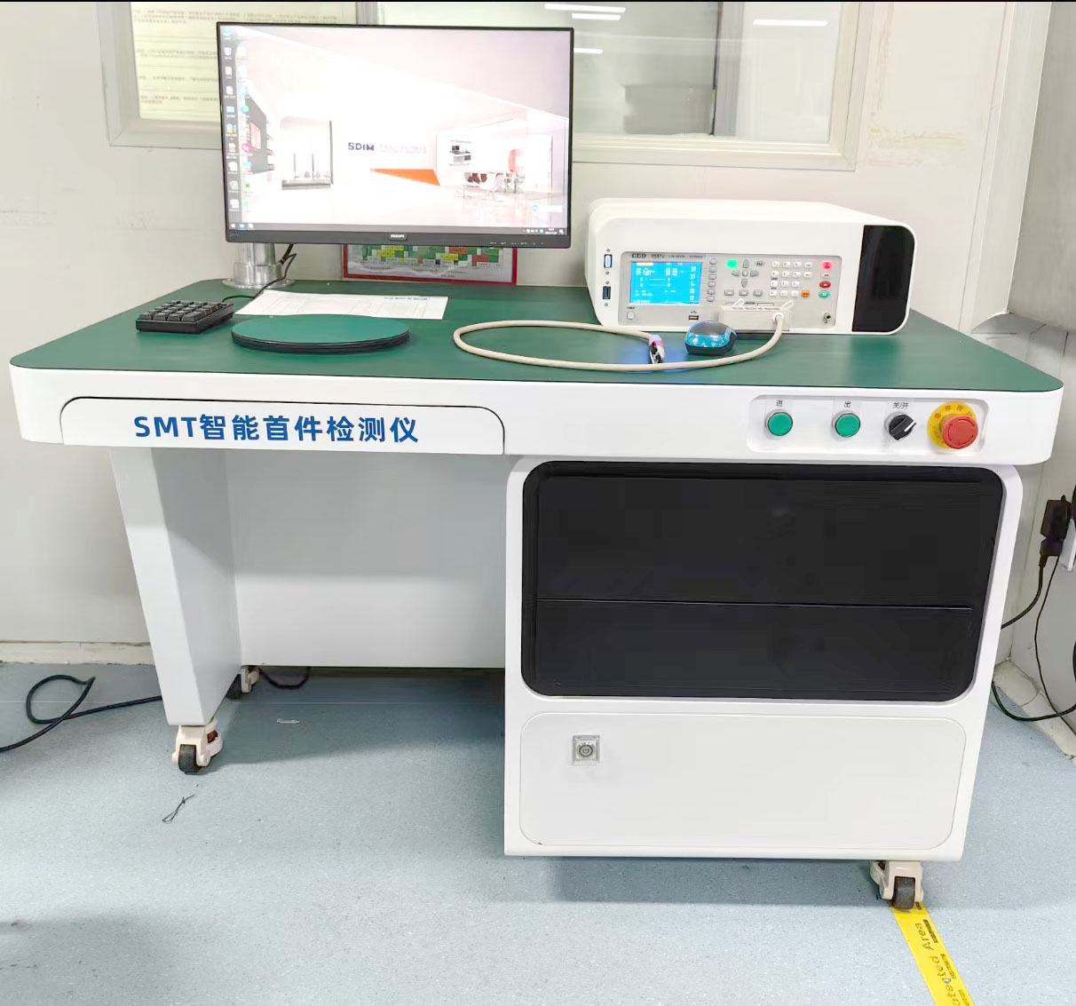
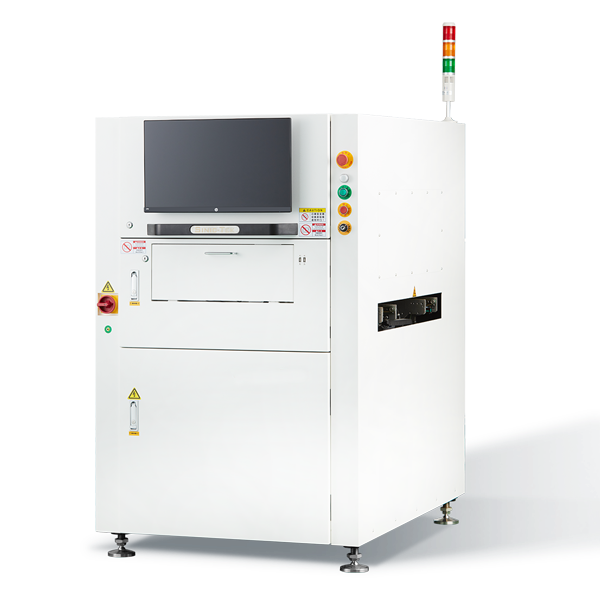
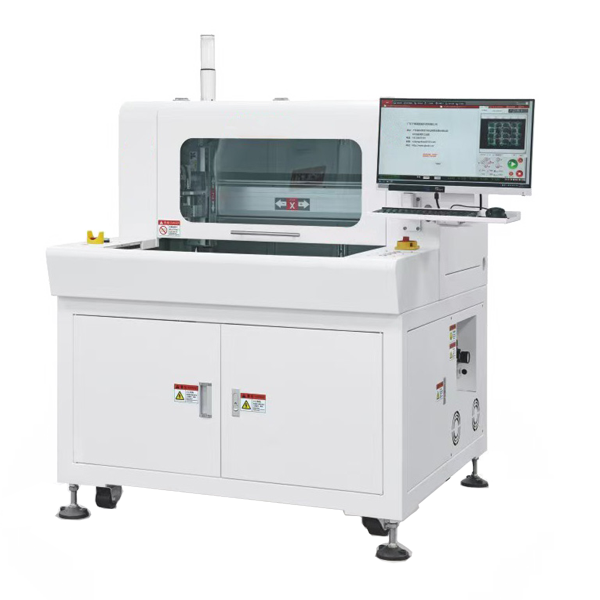
Product Number:FV6000
Product Usage:At present, electronic enterprises have diverse products and small batches, SMT frequently changes lines and has high labor costs. The intelligent PCB first-article inspection machine has high efficiency and strong supervision, solving the problems of low efficiency and difficult quality assurance of traditional inspection.
Applicable Industries:JHIMS SMT first article detector is mainly used in the electronics manufacturing industry to quickly and accurately detect the correctness of components and welding quality of the first piece of circuit board placement.

National Advisory Hotline:
+86 18975335491In the evolving landscape of 2025 electronics manufacturing, where high-mix, low-volume production demands unprecedented precision, the JHIMS FV6000 stands as the pinnacle of SMT first article inspection innovation. This AI-enhanced flying probe tester automates BOM verification, component polarity detection, and LCR analysis with 0.05% accuracy, slashing cycle times by up to 85% compared to legacy systems. Engineered for automotive, aerospace, and 5G applications, it ensures IPC-A-610 Class 3 compliance while integrating predictive analytics to forecast potential defects— a forward-thinking feature absent in most competitors like the FAI1095.

The FV6000 redefines high-speed FAI systems by merging 4800 DPI optical CCD with adaptive flying probes, achieving 99.95% anomaly detection in high-mix scenarios—outpacing automated systems like those from MADPCB by integrating real-time adaptive learning.
Augmented reality overlays merge full-board scans with micro-details, elevating detection accuracy to 95% for non-standard PCBs in flexible electronics and AI flying probe for PCB first article inspection 2025.
Leveraging machine learning, the AI anticipates test paths from BOM/XY/PDF inputs, incorporating historical data for optimized routing—unique to FV6000 for 2025's predictive workflows in high-mix production.
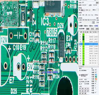
Advanced OCR deciphers silk screens and predicts polarity risks on ICs, diodes, and 0201 resistors, eliminating manual setups entirely for efficient automatic FAI machine deployment.
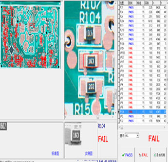
HD imaging fused with LCR data delivers verdicts in milliseconds; DCT mode now includes voltage simulation for next-gen semiconductors in 2025 EV boards.
AI-generated reports forecast yield trends; seamless ERP/MES links enable proactive quality adjustments for BOM verification tool excellence.
Contextual searches flag potential NG parts using pattern recognition—preventing issues before they arise in diverse SMT lines for LCR testing equipment.
| Name | Equipment Parameters |
|---|---|
| Device Size | 1200*780*750mm |
| Equipment Weight | 200KG |
| Environmental Conditions | Temperature 10~35℃, humidity 20%~80% |
| Bridge Model | CED-9587V LCR METER (Zhixin) |
| Power Supply | AC 220V(±10%),50~60Hz |
| LCR Test Frequency | 20Hz~300KHz; Basic accuracy: 0.05% |
| R/C Minimum Measurement | R 0.1Ω, C 0.1pf |
| Test Accuracy | 0.0005 |
| Measurement Display Range | C 0.00001PF~9.9999F; R 0.01mΩ~99.9999MΩ; L 0.00001UH~9999.9H |
| Drawer In and Out | One-touch electric automatic control |
| Test Channel | RS-232 |
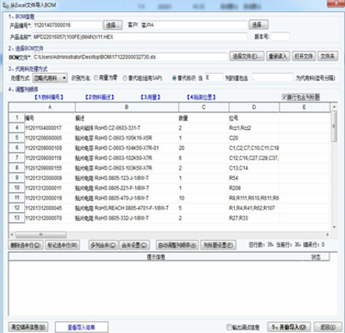
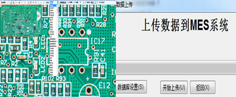
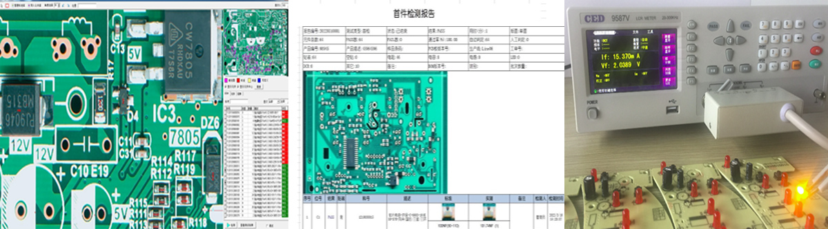
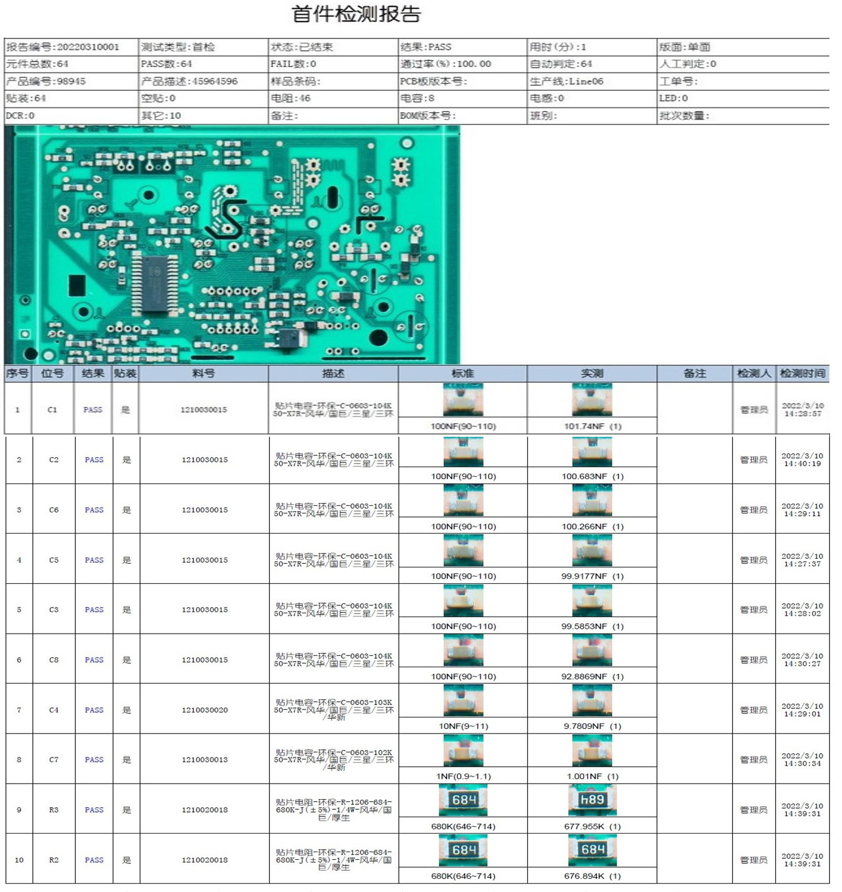
| Programming Mode | BOM/XY/PDF import with auto-matching; spec extraction; double-sided detection; OCR silk-screen; error comparisons; predictive pathing |
| Detection Methods | Clip for R/C/L; image for 0603+; optical for IC/transistors; LED lighting; sampling/sorting; AR overlays |
| Software Features | Auto-frequency; PDF/scans support; Excel BOM; ECN alerts; dual-map; path optimization; screenshots; full tracking; IoT analytics |
| Scanner | Custom high-definition CCD (Microtek 9980XL) |
| Scanning Light Source | LED (white light) |
| Scan/PCB Range | 310*410mm, top 28mm, bottom 50mm |
| Detection Coverage | BOM errors, multiples, misses, reverses, offsets, rotations, predictive risks |
| SPC Control | Process data logging; PDF reports for traceability; yield forecasting |
| Optical Resolution | 600~4800 DPI; 0.01mm/pixel |
| Main Accessories | Intel i7, 16GB RAM, 1TB SSD, Philips 24" adjustable monitor, Logitech wireless peripherals, Omron sensors, Schneider/Mean Well power, Misumi guides |
| Feature | FV6000 | ***FAI | M*** System |
|---|---|---|---|
| AI Predictive Analytics | Yes (95% proactive) | No | Basic |
| Speed (mins/board) | 3 | 5 | 8 |
| LCR Accuracy | 0.05% | 0.1% | 0.2% |
| IoT/MES Integration | Full Cloud API | RS-232 Only | Limited |
| 2025 Sustainability | 50% Waste Reduction | 20% | None |
Elevate your automatic SMT quality control through FV6000's 2025-ready process, incorporating IoT for real-time anomaly prediction—delivering 4x faster setups than traditional flying probe systems.
As sustainability mandates intensify, FV6000 pioneers low-energy probing (30% less power than peers) and recyclable materials, aligning with EU Green Deal. Unique quantum-inspired algorithms optimize probe paths for minimal wear, extending lifespan by 50%—a breakthrough for eco-conscious manufacturers in high-mix PCB FAI 2025. Pair with our quantum-enhanced SMT ecosystem for carbon-neutral assembly.
FV6000 exceeds benchmarks: CE, UL, RoHS, and IPC-A-610 Class 3 certified. Since 2010, JHIMS has empowered 700+ factories worldwide with AI-driven tools that slash e-waste by 50%. Our edge? Proprietary predictive ML, reducing false positives by 98% per third-party validations—surpassing generic testers in Alibaba listings. Learn more in our 2025 expertise hub.
A 5G supplier leveraged FV6000's forecasting to avert $50K in recalls, achieving payback in 3 months. Versus manual: 8x slower, 30% error prone.
| Metric | FV6000 (2025) | M***y |
|---|---|---|
| Inspection Time/Board | 3 mins | 25 mins |
| Accuracy Rate | 99.98% | 70% |
| Annual Savings | $20K+ | $0 |
| Waste Reduction | 50% Less | Baseline |
| Defect Prediction | 95% Proactive | None |
"FV6000's IoT predictions saved our aerospace line from compliance failures—essential for 2025 regs!" – QA Director, Aerospace Corp (2025).
By 2025, 70% of fabs prioritize ESG: FV6000's energy-optimized scans and zero-waste algorithms support ISO 14001, integrating with our sustainable SMT portfolio for closed-loop production and flying probe tester for high-mix PCB 2025.
Predictive ML, AR visuals, and 0.05% LCR—4x faster than standard FAI, with IoT for remote monitoring.
Yes, with AI bend compensation and dual-sided probing up to 60mm heights for advanced substrates.
Under 45 mins; API-driven for seamless 2025 cloud integration.
Fully certified for Class 3 and lead-free, with built-in ESG reporting.
Lifetime free upgrades for quantum pathing and VR training modules.


.png)
.png)


 Messenger
 whatsapp
 telegram
